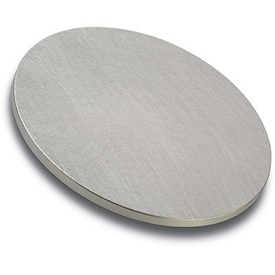
| Material Type | Iron ? |
| Symbol | Fe |
| Atomic Weight | 55.845 |
| Atomic Number | 26 |
| Purity | 3N5-5N |
| Color/Appearance | Lustrous, Metallic, Grayish Tinge |
| Thermal Conductivity | 80 W/m.K |
| Melting Point (°C) | 1,535 |
| Coefficient of Thermal Expansion | 11.8 x 10⁻⁶/K |
| Theoretical Density (g/cc) | 7.86 |
| Ferromagnetic | Magnetic Material |
| Z Ratio | 0.349 |
| Sputter | DC |
| Max Power Density* | 80 |
| (Watts/Square Inch) |
Sputtering is the thin film deposition manufacturing process at the core of today’s semiconductors, disk drives, CDs, and optical devices industries. On an atomic level, sputtering is the process whereby atoms are ejected from a target or source material that is to be deposited on a substrate - such as a silicon wafer, solar panel or optical device - as a result of the bombardment of the target by high energy particles.
The sputtering process begins when a substrate to be coated is placed in a vacuum chamber containing an inert gas - usually Argon - and a negative charge is applied to a target source material that will be deposited onto the substrate causing the plasma to glow.
The sputter yield varies and can be controlled by the energy and incident of angle of the bombarding ions, the relative masses of the ions and target atoms, and the surface binding energy of the target atoms. Several different methods of physical vapor deposition are widely used in sputter coaters, including ion beam and ion-assisted sputtering, reactive sputtering in an Oxygen gas environment, gas flow and magnetron sputtering.
We can help you determine the deposition materials you need to match your physical deposition requirements, and can help you formulate the best alloys and compounds to meet your exact thin film coating specifications.


